Semicolab at IEEE SOCC 2026: independent designs on a shared chip
In Heidelberg, we presented an IHP SG13CMOS5L multi-project architecture connected to Semicolab.
Semiconductor Design


In this article
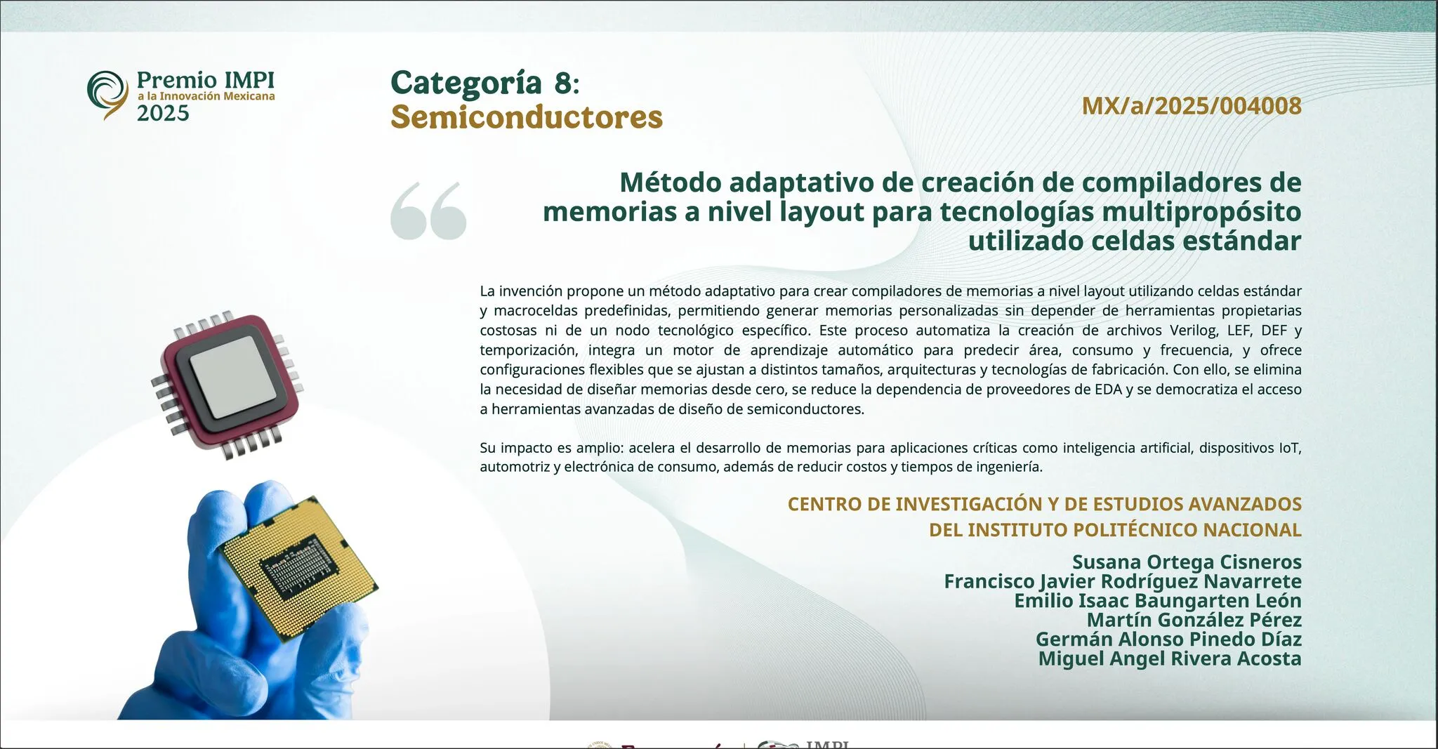
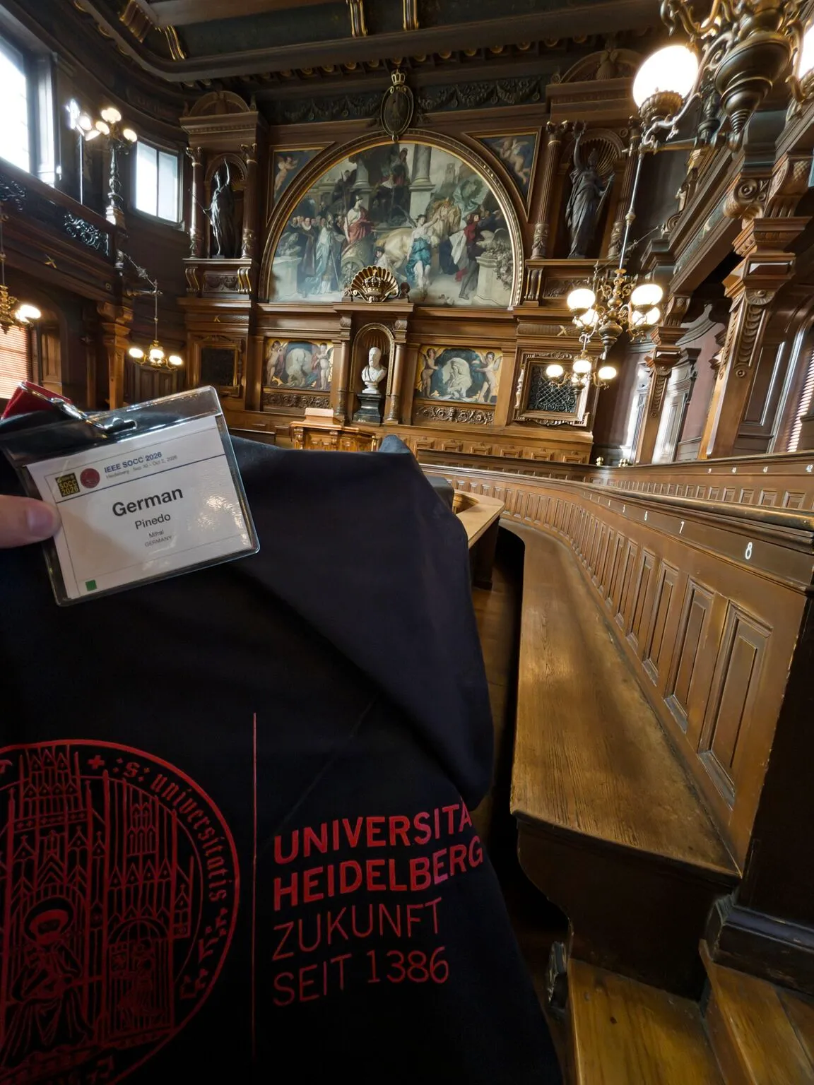
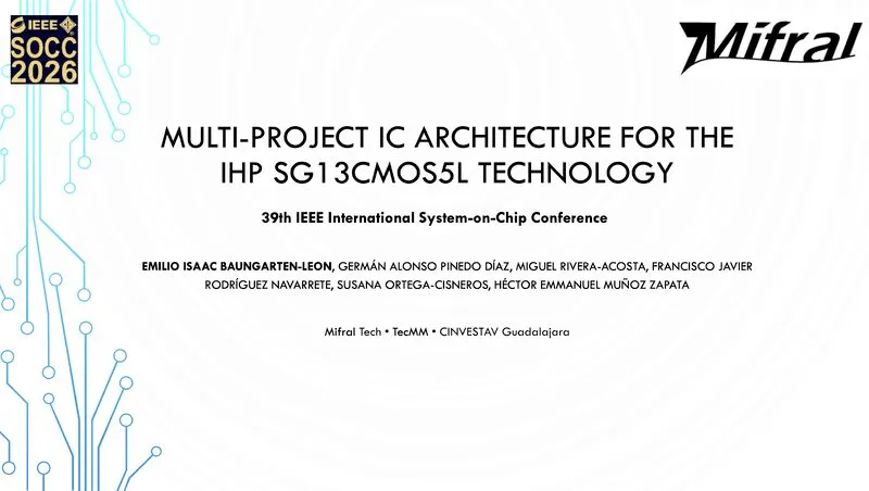
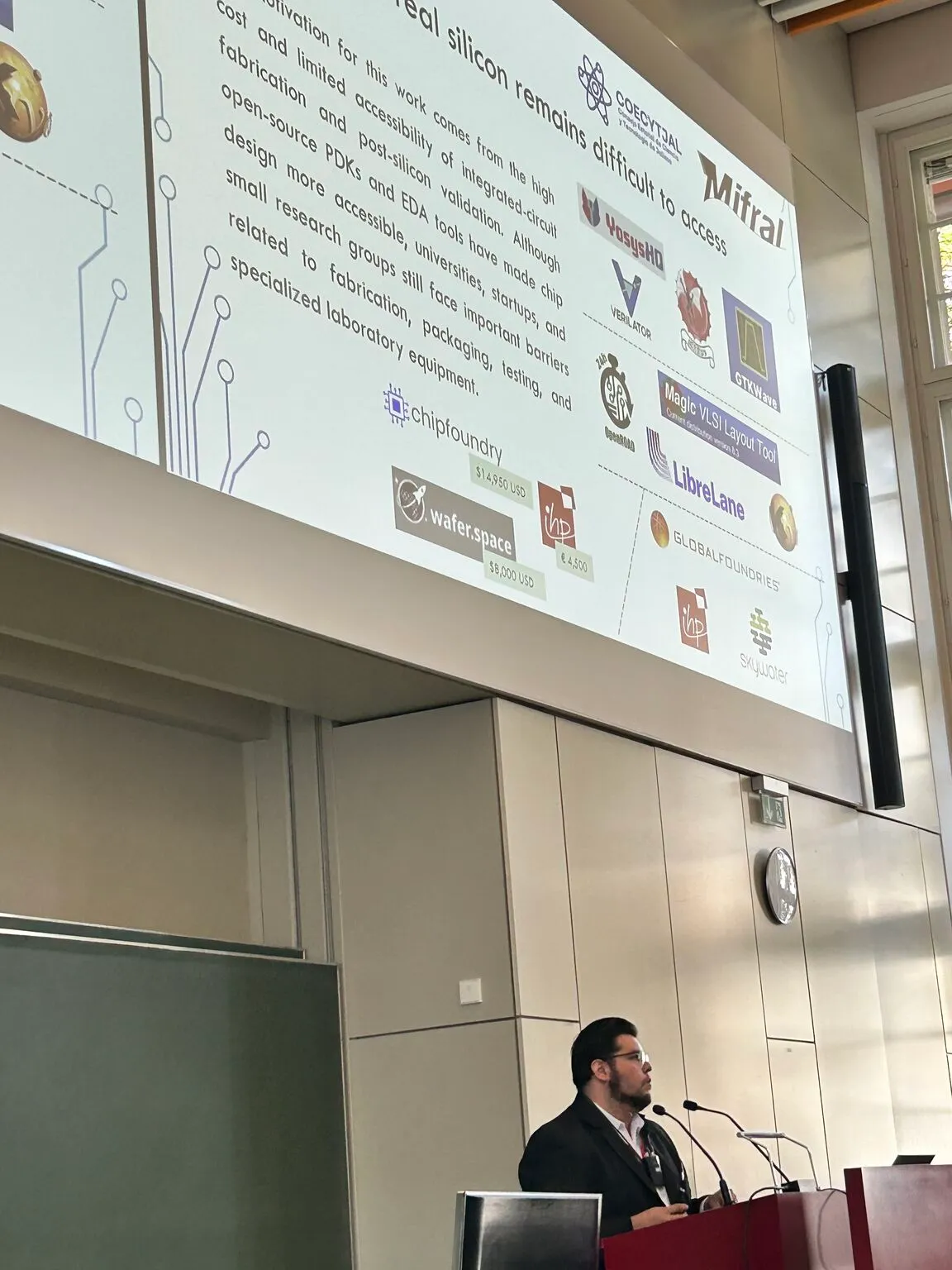
On October 2, 2026, we presented “Multi-Project IC Architecture for the IHP SG13CMOS5L Technology” at the 39th IEEE International System-on-Chip Conference (IEEE SOCC 2026), hosted at Heidelberg University in Germany. The conference ran from September 30 to October 2 in the Neue Universität building.
The work brings together Mifral Tech, TecNM and Cinvestav Guadalajara to address a practical problem: integrating independent designs on one chip and giving them a common way to communicate with a computer. It is one of the development efforts behind Semicolab, our multi-project integrated-circuit platform.
Heidelberg and semiconductor design#
Heidelberg University is a German research university with work in integrated-circuit design. At its Institute of Computer Engineering (ZITI), the Chair of Circuit Design works on mixed-signal chips and sensor-readout circuits for scientific instrumentation and medical imaging. Its work includes simulation, implementation and chip characterization. ZITI Circuit Design research.
Another example is BrainScaleS, from the Electronic Visions group associated with the Kirchhoff Institute for Physics. BrainScaleS-2 combines an analog neuromorphic computing core with digital processing and a communication network on the same chip; BrainScaleS-1 explores wafer-scale integration. These platforms also require software to configure circuits and run experiments. Electronic Visions research.
For our team, presenting in this setting has a direct technical connection to Semicolab: integrating blocks on a chip, controlling them through software and preparing access for training and experimentation.
Sharing the chip infrastructure#
Taking a digital block toward fabrication also requires clocking, reset, communication, registers and external connections. Repeating that infrastructure for every project adds integration work and uses resources that could be shared.
The architecture uses IHP SG13CMOS5L technology to combine multiple user designs, called tiles, within a common harness. Each design retains its own logic and connects through a wrapper with a defined interface. This separation lets teams work on individual blocks before integrating them.
The system shares clock, reset, control and status registers, and an SPI link with memory-mapped register access. A selection mechanism enables one tile at a time, while a multiplexer routes its signals to the external interface. Access control separates harness activation from project selection.
From digital design to layout#
Implementation used Librelane. The individual blocks were verified and physically implemented first, then integrated as hardened macros at the top level. The flow covered synthesis, floorplanning, power distribution, placement, clock-tree synthesis, routing and GDSII generation.
Four digital blocks formed the proof of concept: a 16-bit random-number generator, an 8-bit up/down counter, a PWM generator and a 32-bit logic-operator block. Their functions and requirements differ, but they all use the same connection contract with the shared infrastructure.
What the results show#
Post-layout analysis reports positive timing closure at 100 MHz for the individual macros and 50 MHz for the complete integration. The top level occupies approximately 3.24 mm² and contains 5,033 standard cells. Based on the cell counts reported in the paper, the shared harness accounts for 1,171 cells, or 23.3% of the logical total.
These figures describe the implementation and post-layout analysis in the paper. They are not measurements from a fabricated chip. They help assess integration and resource overhead before physical silicon characterization.
The connection to Semicolab#
The Semicolab graphical interface is intended to let users select a project, configure inputs and registers, and inspect outputs from a computer. SPI communication translates these actions into reads and writes on the circuit. This makes it possible to work with registers and buses without providing a separate physical connection for every design signal.
At Mifral, we are connecting that design and interaction flow with technical training, research and prototyping. A common interface can help different teams share a testing platform and focus on the circuit they are developing. Compatibility with the graphical interface is part of the presented work; validating the complete system on silicon requires its own tests.
The AI-generated illustrations show a conceptual workflow and a possible six-project interface. They do not document fabricated hardware or a working application; the paper’s results refer to the four blocks described above.
Semicolab remains in development. This story documents the presented architecture and its connection to the platform. Its product page will be added to the Products section when it is ready.
Joint work and participation#
The paper is authored by Emilio Isaac Baungarten-Leon, Germán Alonso Pinedo Díaz, Miguel Rivera-Acosta, Francisco Javier Rodriguez Navarrete, Susana Ortega-Cisneros and Héctor Emmanuel Muñoz Zapata, with affiliations at Mifral Tech, TecMM and Cinvestav. We thank COECyTJAL for supporting the team’s participation in IEEE SOCC 2026.
The presentation in Heidelberg gave us an opportunity to discuss this implementation with the system-on-chip design community. We continue to develop the connection between the circuit, access tools and Semicolab training resources.
Sources and context#
From concept to Heidelberg
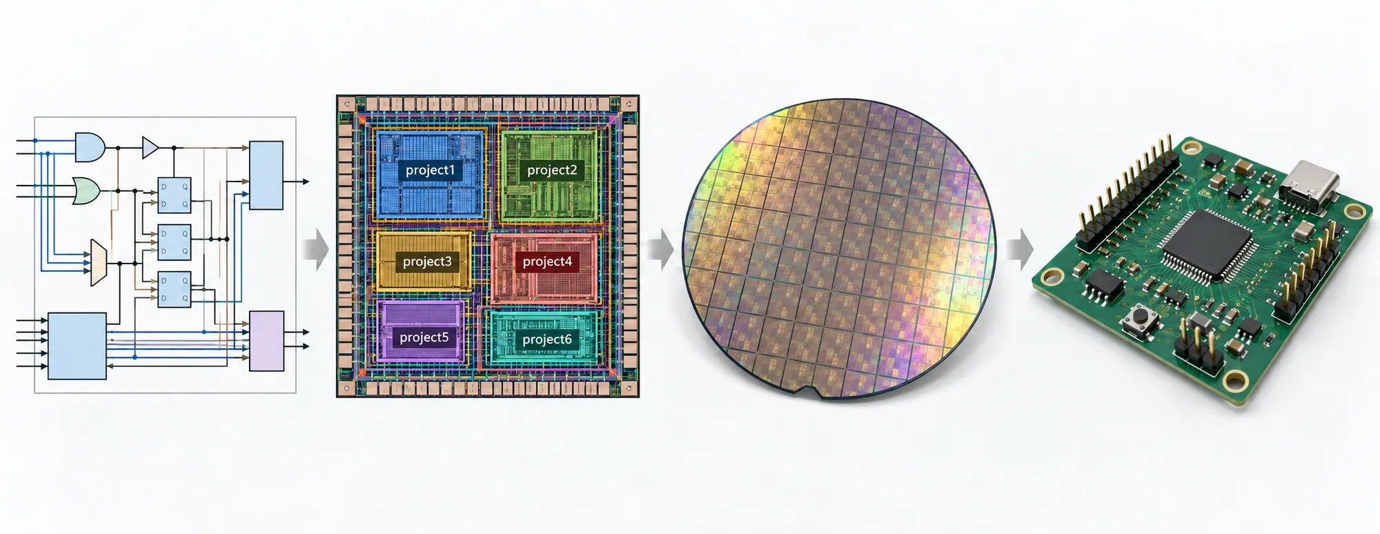
AI-generated image
Concept illustration created with ChatGPT. It is not a photograph of fabricated hardware or a screenshot of a working application.
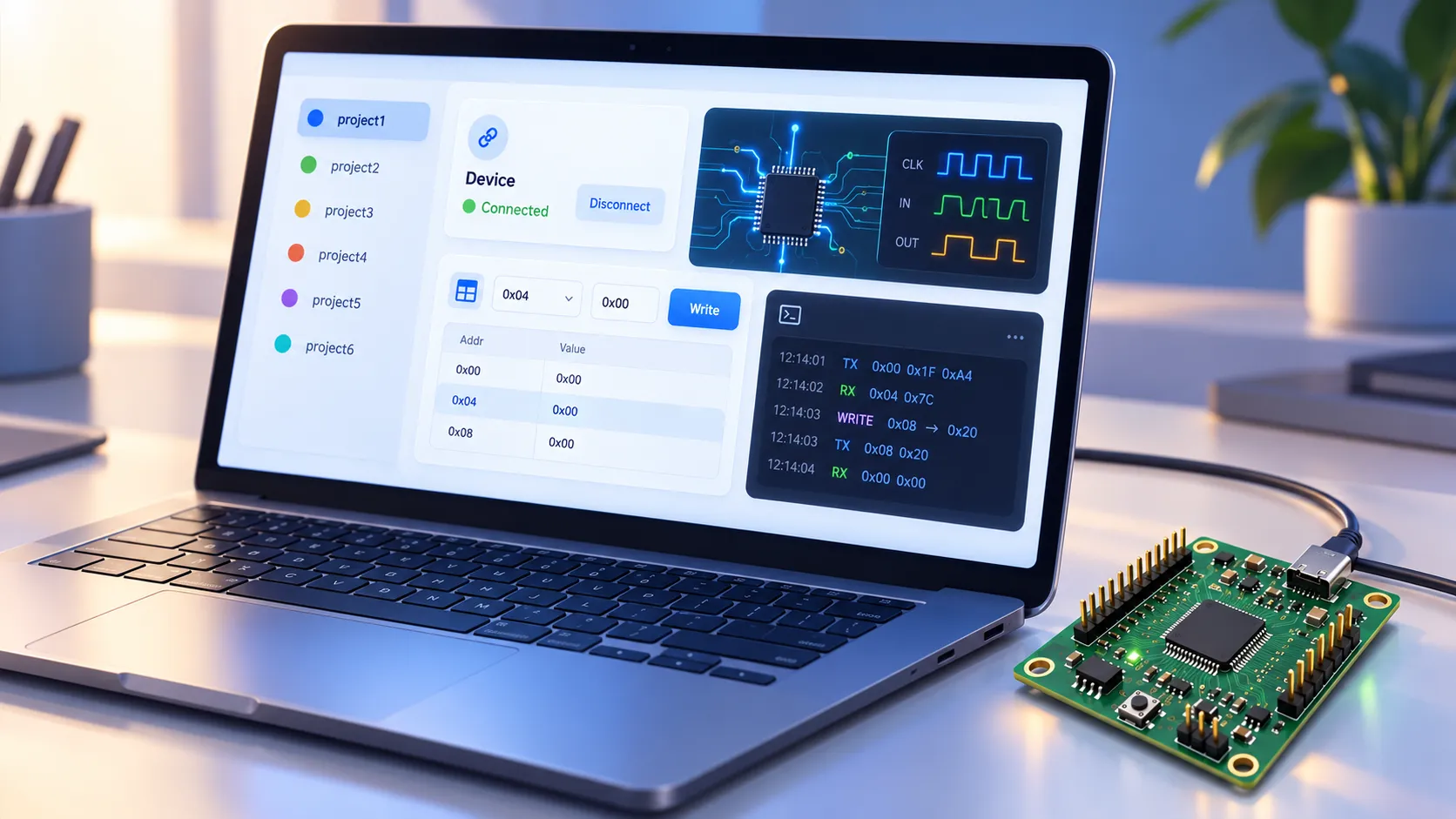
AI-generated image
Concept illustration created with ChatGPT. It is not a photograph of fabricated hardware or a screenshot of a working application.

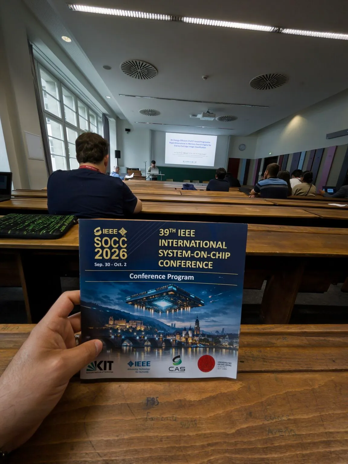
Research paper
Multi-Project IC Architecture for the IHP SG13CMOS5L Technology
IEEE Xplore link pending. We will add it when it becomes available.